Dec 9 2004 4 V. Power Consumption and Supply Voltage 2.

Schematic Of The Proposed Lna Download Scientific Diagram
Low Noise Amplifier inductor cadence.
. Lna design tutorial cadence The Cadence IC has a lot RFIC design examples. RelXpert is a tool developed by Cadence to simulate MOSFET devices for device degradation due to various reliability mechanisms like HCI NBTWBTI etc. Work is done one the Cadence virtuoso platform using the tsmc18 library.
Designed Cascode LNA is implemented in cadence virtuoso platform using 65nm technology with gain of 15dB. While the design of LNA is being made with wireless. Design of a 10GHz LNA for Amateur Radio Operation Using AWR Software Cadence is a pivotal leader in electronic design and computational expertise using its Intelligent System Design strategy to turn design concepts into reality.
Look at the Cadence document and the example. In this study we have analyzed key building blocks used in RF receiver front-end such as Cascode and Folded-Cascode LNA amplifiers Cross-coupled LC VCO and Mixer using Cadence RelXpert and. This paper addresses Low Noise Amplifier design which is also known as LNA for any application in wireless communication system.
The fabricated LNA chip is packaged and tested. The specifications of LNA design are indicated in Table 3 Table 3 Specifications Of LNA Design6 5. You will be familiar with the Cadence RFIC design tool.
The LNA provided a reasonable gain which was 1453 dB. 5-GHz CMOS low noise amplifier IEEE Journal of Solid State Circuits Vol32 May 1997. Any one help me that i am doing Complemetary current reuse LNA in MICS band in Cadence spectrai selected one IEEE paper regarding my projectIn that they didnot mention any device specification ie value of.
In this paper we design and Simulate Low Noise Amplifier using Cadence Virtuoso R. The measured results gain noise figure and IIP3 correlate with the simulation very well. Maintain this current density throughout the rest of the design steps.
They layout is also design with zero errors in both the Design Rule Check DRC and Layout vs Schematic check LVS implying that the design is ready for fabrication. LNA DESIGN USING SP ANALYSIS Starting with W f 1μm N f 80 Start with ballpark values for the inductors from hand-calculations First tune L S to obtain R in real part of ZM 1 close to 50Ω Next tune L G to center S 11 null at f 0 Tune L D to center the peak of S 21 at f 0 L G L S L D. Vonleo Member level 1.
In this paper a low voltage CMOS LNA is designed for the GPS L1 band. Heterojunction Bipolar Transistor HBT LNA The design of the LNA is a cascode stage driving an emitter follower with a resistive feedback. This is equivalent to solving.
Joined Oct 30 2004 Messages 34 Helped 1 Reputation 2 Reaction score 0 Trophy points 1286. The schematic was implemented in Cadence Virtuoso Schematic XL using the generic processing design kit GPDK 45 nm library and was simulated using Analog Design Environment ADE. 1dB compression point 1-dB of -2847dBm with a low power consumption of 49µW.
Welcome to the RF Design Tutorials video tutorial series. Determine the J OPT of the amplifier. RFDESIGN 2008 over 10 years ago.
The simulated results are obtained and compared with earlier work as shown in table 1. A 15GHz-20GHz Low Noise Amplifier LNA is designed in IBM 018um BiCMOS technology using IBM design kits in Cadence Design Flow. A Low Noise Amplifier is the basic building block or key component in the Communication System.
Design Methodology for CS and Cascode LNA I Step 1. It can be used for receiver with. 43 Design Specification Of LNA There are some important specifications that LNA should achieve.
To characterize the LNA following figure of merits are usually measured or simulated. Pad capacitance and parasitic capacitance of L B reduce input impedance Tail current source in diff-pair adds noise and common-mode instability. The results demonstrate that IBM SiGe technology.
LNA design is a compromise among power noise linearity gain stability input and output matching and dynamic range. The following graphs shows S21 S11 noise figure IIP3 of. Clarification on LNA design.
Tuned LNA design notes MOSFET LNA design usually compromises noise figure for power dissipation low-noise current is too high In this approach linearity increases with Z O. These factors are characterized by the design specifications in. Any Radio Receiver is made from Low Noise Amplifier mixer and Filter Power Efficient Active Filter where LNA plays a challenging role of amplificati on in the Radio Receiver Circuit.
DISCUSSION AND RESULTS Design and analysis of low noise amplifier is designed and simulated by using CADENCE software with latest technology 013µm. In case of CS stage use V DS V DD I Step 2. In this paper we proposed a low power low noise amplifier LNA dedicated to biomedical applications.
The cascode circuit is useful because it provides a larger gain and makes a stronger circuit. Cadence customers are the worlds. Start cadence by typing ams_cds tech c35b4 mode fb Make a new library RF_LAB1 in Cadence Library Manager Create and draw the Schematics.
CS LNA with inductive source degeneration. The LNA presented in this thesis achieved the lowest power consumption of 101 mW with a supply of 1 V. Proposed design of LNA 66 Simulation Results The proposed design is simulated over Cadence spectra 018μm CMOS technology with 18V supply voltage.
Set the V DS of transistor for maximum linearity such that clipping of output is avoided. Common Source CS LNA. FminJ J 0.
The emitter follower is used as a buffer and provides more power and current to the circuit. In the 9th video of the series you will learn about practical RF Low Noise Amplifier design flow. The standard CMOS technology has revolutionized the transceiver circuits in communication systems.
The lab is based on a Cadence SpectreRF Workshop session and its manual LNA Design Using SpectreRF previous called Application Note which is found on the course page. According to the configuration the CMOS LNA design can be classified as follows. The design was simulated using the ADS and also cadence tools provided for the 013 m RF CMOS process.
Narrow-band LNA is the building block of any such CMOS-based receiver. Community Forums RF Design clarification on LNA design.
2
12 16ghz Lna

Seeking For Help In Pss Analysis Rf Design Cadence Technology Forums Cadence Community
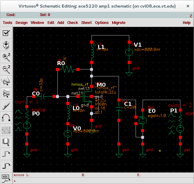
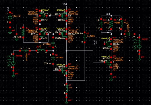
Linear Simulation For An Amplifier Multifunctional Integrated Circuits And Systems Group Mics Virginia Tech
2

Figure 7 From Design And Analysis Of Low Noise Amplifier Using Cadence Semantic Scholar

Figure 1 From Adaptive Enhancement Of Low Noise Amplifier Using Cadence Virtuoso Tool Semantic Scholar

Figure 2 From Adaptive Enhancement Of Low Noise Amplifier Using Cadence Virtuoso Tool Semantic Scholar
0 comments
Post a Comment